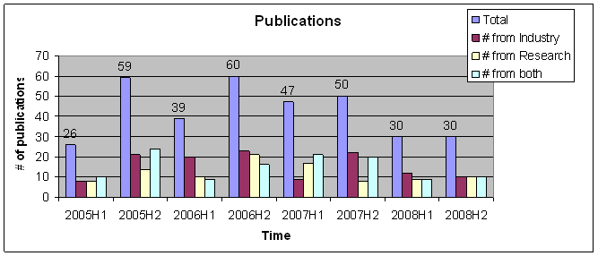
In general: Many, many publications and contributions to conferences, workshops, forums, …
EXAMPLE 1: SIP test strategies

Figure 1: SiP in stacked die technology |
In the course of the project, a strategy for testing SiP products has been developed and rolled out to the business divisions. The strategy is supported by a set of SiP test development guidelines. These guidelines contain all the important information for planning and implementing SiP tests in order to achieve the outgoing quality and cost targets, and to have the SiP “first time right”. The main topics covered by the guidelines are: Test and Analysis of Dies inside a SiP, SiP Structure Test, Boundary Scan Implementation, Test Verification, Test Program Assembly & Reuse, and Customer Requirements with respect to PCB Test. Several guideline updates and refinements cover the latest insights and practical experiences. |
Development steps:
2005: SiP test requirements definitions, known good die (KGD) and delivery quality, SiP cost calculator
2006: Concept and implementation of SiP high speed interconnect test, on-chip resources for pattern generation and analysis, loop-back test, pilot project in wireline communications. Paper on “SiP test strategies” at ETS ‘06
2007: SiP Test Guidelines definition and roll-out in business units, update of SiP cost calculator
2008: Full implementation and optimization of SiP test strategy, refinement of SiP test guidelines
The SiP Test Strategy and DfT Guidelines have turned out to be very helpful to manage the test and quality issues in complex SiP design projects.
EXAMPLE2: DFT for RF Mixed-signal components: SD converters
State-of-the-art:
In order to satisfy the rising demand for high-quality audio devices, the performances of Sigma-Delta Analogue-to-Digital Converters (ΣΔ ADCs) are continuously improving with larger modulator bandwidths and higher dynamic ranges. As the performances of these circuits increase, its test is in turn more difficult and costly. Built-in Self-Test (BIST) techniques can reduce this cost by integrating the test approach in the design. A first technique for the BIST of ΣΔ ADCs was proposed by Toner and Roberts in 1993 [1]. In that proposal, a binary stream generated by an on-chip ΣΔ-based digital oscillator was applied to the input of the converter. Several strategies were considered to analyze the output response on chip, all of them leading to a large hardware overhead. More recently, in [2] an attenuated binary stream generated by a software-modulator was used to test a 2nd order modulator but still analyzing the output response was not considered on-chip.
[1] M.F. Toner and G.W. Roberts. “A BIST Scheme for an SNR Test of a Sigma-Delta ADC”, in Proc. IEEE International Test Conference, Baltimore, USA, pp. 805-814, Oct. 1993.
[2] C.K. Ong, K.T. Cheng, L.C. Wang. “A new sigma-delta modulator architecture for testing using digital stimulus”, IEEE Transaction of Circuit and System I, V. 51, pp. 206-213, Jan. 2004.
Link to ITRS (2004-2005 Edition):
The 2004 Update, page 29, recognizes as a difficult challenge for highly integrated designs for nodes >45nm/through 2010 : “Analog DFT and BIST techniques must mature to simplify test interface requirements and slow ever-increasing instrument capability trends” and “Testing chips containing RF and audio circuits will be a major challenge if they also contain large numbers of noisy digital circuits”.
Successful results:
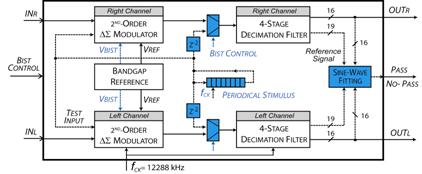
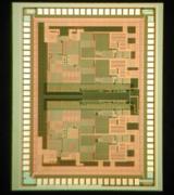
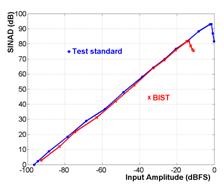
We have developed a new architecture (Figure 1.a) for audio ADCs that includes a BIST technique for the test of the Signal-to-Noise-plus-Distortion Ratio (SNDR). A periodical binary train is integrated in the chip in order to stimulate the converter. The reuse of the bandgap circuit already existing in the converter allows us to generate the test stimulus with a very small analogue overhead area. The output response analysis is performed by means of a sine-wave fitting algorithm. The reuse of the digital filter already existing in the converter allows us to generate a synchronized reference signal necessary for the fitting-algorithm. Therefore, the digital overhead area is dramatically reduced. The BIST technique is equivalent to a standard test carried out with a sinusoidal signal at ‑12 dBFS. The ΣΔ BIST was validated in silicon using a 0.13 m CMOS technology from STMicroelectronics in 2006 (Figure 1.b). This BIST technique is targeted primarily to reduce production test costs. The purely digital blocks were emulated by means of Matlab. The estimated BIST overhead area is 7.5% of the whole stereo converter area. This was the first silicon validated BIST principle that used purely digital tests. Figure 1.c shows the SNDR measured with a standard test and with the BIST technique. The error is very small (always smaller than 2 dB) for input amplitudes up to ‑12 dB. As expected by simulation results, for higher amplitudes the high-frequency quantization noise of the binary stimulus causes the saturation of the converter and the SNDR degradation. Additionally, for input amplitudes between ‑60 and ‑12 dBFS, the error is smaller that 1dB. Work is on-going towards the industrialization of this technique.
[1] L. Rolíndez, S. Mir, J.L. Carbonero, D. Goguet and N. Chouba. A stereo audio ADC architecture for embedded SNDR testing. IEEE International Test Conference, Santa Clara, USA, October 2007.
[2] L. Rolíndez, S. Mir, A. Bounceur and J.L. Carbonero. A BIST Scheme for SNDR Testing of ADCs Using Sine-Wave Fitting. Journal of Electronic Testing: Theory and Applications, Springer Science+Business Media, 22(4-6), 2006, pp. 325-335.
Impact on Standardisation: Facilitates the test of Sigma-Delta converters by using purely digital tests that can be interfaced via digital test standards such as JTAG.
Focus on NanoTest metrics (TTM, Quality and/or Cost): Test cost is reduced by eliminating the need of mixed-signal testers. Test time can be reduced by a factor of 10: the total test time is about 60 ms, while traditional tests requires times close to 1 second (for the considered case-study).
 |
(a) |
|
|
(b) |
(c) |
Figure 1. (a) Self-testable 16-bit Stereo ΣΔ ADC Architecture, (b) fabricated circuit and (c) SNDR measured by standard and embedded testing. |
EXAMPLE 3: Feasibility and functionality of a full set up of BIST/BISR including high-end ADC with full compensation bench
This complete system (see the flowing figure) is realized with a 14bit DAC (80 MSPS clock) for stimuli generation, the 12 bit ADC (80 MSPS) and the associated process unit in FPGA.
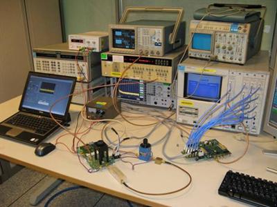
In the first step, the embedded DAC is used to generate a sinewave into the ADC input. According to the ADC response a LUT (look up table) is filled. This LUT holds the code modifications allowing the best correction of the ADC linearity. After this initialization phase, the pair ADC-LUT can be used as standalone ADC.
In order to evaluate the efficiency of the compensation the ADC and ADC-LUT responses are captured for a single tone input signal provided by an external generator
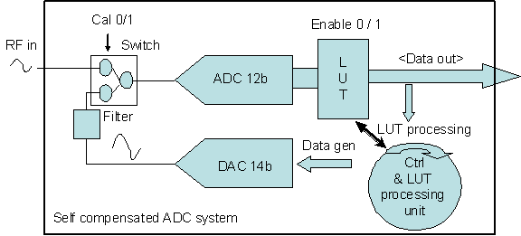
The next figure shows a the frequency response of the ADC without and with (ADC+LUT) the compensation:
The auto-compensated system is functional at speed and provides good performances.
The main contributor in our set up is the H3 (third harmonic) and the compensation provides 10dB improvement (see following table)
Harmonic |
Before compensation |
Compensation enable |
H3 |
-78,15 dBc |
-88,56 dBc |
Some of the key results were presented on a Poster during the European Nanoelectronics Forum 2008.
Executive Summary [project results over period 2005-2008]
- WP2 and WP3 goals achieved, methods ready for production
- WP1 activity successfully transferred to NXP-NL
- Several innovative methods and tools developed, and ready for deployment through the organization
- Very fruitful cooperation with LIRMM, TIMA, and NXP-NL
- Creation of ISyTest (Institute for System Testing), a joint institute with LIRMM
18 publications, 2 Awards |