General goals
In the period 2005 2008, the CMOS technology 65nm will become available and 45nm will be developed. Furthermore, process options will be developed for 90nm. As documented in the ITRS roadmap , these new technologies impose new challenges on test methodology, triggered by an increasing number of gates per chip, smaller dimensions and new defect mechanisms. This is a real challenge, since the complexity of test-generation grows exponentially with the number of gates . With todays test methodology, it will not be possible to achieve a high test-coverage and fast ramp-up at acceptable cost. This is confirmed by the Medea+ Design Automation (EDA) Roadmap , identifying nine areas for test innovations.
The European microelectronics companies AMIS, Infineon, NXP and ST intend to strengthen and realign their efforts dedicated to testing spent in Medea+ phase 1. They recognized that it is most efficient to build from the results of the projects Technodat and Associate in a single, focused project, NanoTEST, under Medea+ phase 2. The consortium is a mix of five large firms, two SMEs and three institutes. This guarantees efficient know-how transfer from academic research and industrial R&D down to production level, e.g. at ST/NXP/Motorola fab in Crolles (F), Infineon fabs in Villach (A) and Corbeil-Essonnes (F), NXP fabs in Nijmegen (NL) and Caen (F), AMIS fab in Oudenaarde (B).
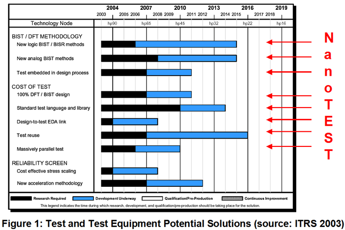
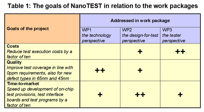
NanoTEST will directly contribute to the commercial success of the European microelectronics industry in applying their new wafer and packaging technologies, targeting not only system-on-chip (SoC), but also system-in-package (SiP). It addresses two of the three identified areas of potential solutions of the ITRS test roadmap (see Figure 1). It will create breakthroughs in test, in the area of costs as well as achieved quality and time-to-market. The activities are split in three discipline-orientated work packages addressing the technology, design-for-test and tester disciplines, respectively (illustrated in Table 1).
This will result in:
• Reducing the cost of production testing by a factor of ten. The way to achieve this ambitious goal is to develop new methodologies that enhance tester throughput and reduce tester resources. For example, multi-site testing, low-cost test cells, advanced test interface boards, and test resource reduction by on-chip test provisions that go much further than current design-for-test practices. It is key now to determine the optimum balance between on-chip test provisions and off-chip test equipment.
There is a growing market trend towards heterogeneous systems like SiPs in situations where this is more economical than a single SoC. This project also intends to reduce production test costs of SiPs. Issues to be addressed are for example test provisions for intra-package access and inter-die testing, wafer probe technologies, signal integrity issues affecting test, and development of standards.
• Improving the quality of test, despite the fact that occurrence of new defect types in 65nm and 45nm will initially drive the defect levels up. This will be achieved by developing test methodologies for new defect types, as well as extending the use of tester data into the domain of fault diagnosis for fast production ramp-up, characterization and self-repair. Delay fault test strategies play an essential role in covering new defect types. The work on diagnosis will provide the necessary feedback to zero-defect programs, driven by the automotive sector.
• Speeding up the complete design-for-test and test program generation flow by a factor of ten. This challenging goal can be achieved by deploying re-use at the optimum abstraction level. At the same time new methodologies will be developed for future designs, containing for example globally-asynchronous-locally-synchronous circuits, volatile and non-volatile memories, RF, mixed-signal blocks and sensors. Furthermore, tools will be developed to automate mixed-signal test specification and test program generation.
Strategic relevance (relevance for Europe)
This project relates to the following work areas of the Medea+ program : 1.7.14, Test development for SoC and SiP, 2.1.6, Test and characterisation, 2.2.4.3, Test and test equipment for memories, 2.2.5.3, Test and test equipment for RF. It supports the European efforts towards a leading position in microelectronics and a commercial success of the future technology nodes 65nm and 45nm. Designs in those technologies will not only contain logic but also process options such as memories, analogue and RF. This project is indispensable to design and manufacture complex products in a short time at market compliant cost.
System companies are imposing tough quality requirements on the microelectronics companies, even as a technology node is still maturing. Common quality requirements are 100ppm or less, while the manufacturing yield is typically lower than 90% (equivalent to 100,000ppm). Testing plays an important role in meeting quality requirements. On one hand, testing filters out defective parts, which is the traditional role of manufacturing test. This provides the enabling technology to bridge the gap between manufacturing yield and quality requirements. On the other hand, testing provides feedback on weak spots to the process and design teams. This is an emerging role of manufacturing test. It provides fault observability to support faster ramp-up. Not only SoCs and their building blocks are addressed, heterogeneous systems like SiPs are included as well.
The consortium will benefit from European cooperation by sharing the results, between institutes and industry, but also mutually between the large firms. Together, the consortium has more weight towards ATE and EDA vendors, and in standardisation initiatives.
State-of-the-art (technical background)
Present situation in the field
Testing has become a major concern in the microelectronic industry as testing costs keep growing, claiming a growing percentage of the total device manufacturing cost. Typical test costs as a percentage of the manufacturing costs are around 5-10% for logic, 10-30% for mixed-signal and can be as high as 50% for products with embedded RF. The main reasons are the growing device complexity enabled by new wafer fab and packaging technologies higher cost-of-ownership of ATE equipment and longer test execution time per chip, as well as customer requirements for shorter time to market and higher product delivery quality. In line with the work package structure of this project, the present situation is now discussed from three perspectives: technology, design-for-test and tester.
The technology perspective: New defect types will appear in the new technology nodes, requiring new test methodologies. Understanding failure mechanisms and process/parameter shifts is supported by feedback of tester data from the test floor to the engineering environment. This is also known as yield learning. The semiconductor industry is just beginning to explore the potential and appreciate the benefit of this; current practice is not yet mature. The feasibility and validity of the current diagnosis and fault localization methods and tools have been successfully demonstrated on yield monitors but their usage still requires specialist-skills. In order to make them easier usable in the field on a broad range of products, further improvement is needed. The application of delay fault test methodology has also not yet fully matured and the (delta) Iddq test method is approaching its limits. Replacements must be found in the form of novel defect-based test methods targeting logic, memory, mixed-signal and RF, as well as sensors. Further, safety-relevant application in the automotive area requiring extremely high quality levels must be addressed by advanced test and screening methods (zero defect programs).
The design-for-test perspective: Design-for-test (DfT) offers powerful techniques to reduce product cost and test complexity. It offers the on-chip infrastructure to perform the tests demanded from the technology perspective. For digital designs, such techniques are much more advanced than for analogue, mixed-signal and RF designs. Examples are modular test and test wrappers standardised under IEEE1500. Although some mixed-signal DfT techniques have been proposed in recent years, they have so far failed to get wide industrial acceptance. The digital domain needs a major step in the development of DfT techniques as well, for example by introducing the use of DfT constraints during the design flow, and new techniques for test resource reduction. This is mainly caused by the growing data volume to be handled by the tester. The growing use of SiPs will drive the need for new design-for-test approaches focusing on intra-package access and testing.
The tester perspective: Dramatic improvements in the area of test engineering are considered indispensable to keep production test costs in-line with market prices. The costs are strongly influenced by the required tester memory size and tester features. Multi-site testing, BIST, advanced wafer probe card technologies will play an important role here. Special attention must be given to the test cost of products that go into low-priced consumer applications. Data sizes to be handled by the tester are growing and test frequencies go up. This becomes unmanageable if nothing is done about it. The link from design to the tester platforms should be improved by making use of standardization on STIL/CTL. Pure ATE aspects are outside the scope of the project (e.g. development of ATE equipment).
Innovations proposed
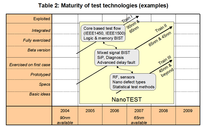
NanoTEST will address completely new test challenges but will also further extend still immature methods explored in previous projects to enable the full exploitation in products outside this project (already during the runtime of NanoTEST). This is illustrated by the three trains in Table 2, showing a few examples of the current maturity of test technologies. Train 1 is targeted at 65nm introduction and 90nm maturing (incl. process options like mixed-signal). Train 2 is targeted at 45nm introduction and 65nm maturing. Train 3 is targeted at 45nm maturing and beyond. The test technologies are not independent. For example, mixed-signal BIST relies on core-based test access and control.
The work in this project is split in three discipline-oriented work packages. WP1 investigates what defects occur in new processes and develops methods to measure those defects. WP2 addresses what needs to be done in the design in order to perform the tests, and fits this into the design flow. WP3 decreases the cost of testing by capitalising on the results of WP1 and WP2, and by automating the test program creation flow.
The technology perspective, addressed in WP1:
This work package addresses the areas 14.3, defect oriented testing, 14.6, failure analysis and diagnosis, and 14.7, on line testing and fault tolerance, of the Medea+ EDA Roadmap . The innovations proposed are:
- New fault models and implementation of novel defect-based test methods.
- Application of these methods in an early stage of ramp-up in the fab (yield learning).
- New structural test methods for logic, memory, mixed-signal and RF.
- Extension of memory BIST: characterization, diagnosis and self-repair capability.
- Test and diagnosis of dynamic faults and delay faults.
The design-for-test perspective, addressed in WP2:
This work package addresses the areas 14.1, core testing, 14.2, high-level test synthesis, 14.4, automatic test program generation, and 14.9, system in package, of the Medea+ EDA Roadmap. The innovations proposed are:
- Access and control concepts to perform the novel defect-based test methods developed under WP1.
- Test flow based on design constraints and RTL level infrastructure IP blocks such that it can be applied in modern design-synthesis flows.
- Minimise the costs by the right balance between on-chip (WP2) and off-chip (WP3).
- New techniques for test resource reduction, e.g. reduced pin count test, test data compaction, built in self-test and oscillation testing.
- DfT library of on-chip test provisions for embedded analogue, mixed-signal, RF,
high-speed I/O, FPGA, volatile & non-volatile memory modules, sensors.
- Core-based test approach for mixed-signal blocks. Develop Mixed-signal BIST and BOST for high-resolution ADCs.
The tester perspective, addressed in WP3:
This work package addresses the areas 14.5, test development for SoC, of the Medea+ EDA Roadmap. The innovations proposed are:
- Advanced test interface board and wafer probe card technologies with higher probe count, frequency, signal integrity and power capabilities.
- Multi-site testing for mixed-signal & RF.
- Optimisation of the cost for a testability solution by combining DfT, BIST,
built-out-self-test (BOST), wrapper-based mixed-signal modular test, and tester instrumentation for various functional blocks, e.g. high-speed I/O, memory,
mixed-signal, RF. This will enable the use of low-cost test cells.
- Test specification and program generation tools to support the new cost-cutting test approaches (making use of techniques developed under WP1/WP2 and standards).
- SiP test methodology based on a known-good-die approach, involving the innovations to find the cost minimum between chip-level and package-level test efforts.
- Defect models for sensors, addressing new physical domains like magnetic fields.
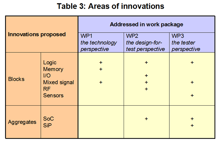
Table 3 summarises the areas of activity in this project.
Main competitor announcements
Competitors also feel the need for in-house innovation in the area of test. This was confirmed in the Die Products Consortium meeting during ITC 2003, where Intel, IBM and others presented their needs for quality test flows in general and delay fault test in particular. It was remarkable how similar the test problems are and that all companies are working on proprietary solutions, in-house tools, scripts and libraries, additional to commercial solutions. The commercial EDA and DfT vendors are not expected to offer full solutions at the time that the European microelectronics companies in NanoTEST need them, caused by our aggressive technology roadmap for 65nm and 45nm. For example, software tools for core-based testing (e.g. Synopsys) do not support analogue, mixed-signal and RF test. The same is true for diagnosis of dynamic faults, delay faults in memories and for test of SiPs.
Thus, for a successful implementation and mass production of products in 65nm and 45nm, microelectronic companies need to work on their own test technology additional to commercial EDA tools.
Previous / complementary activities of the partners in the field
This project will benefit from previous European co-operations (e.g. Medea A401 & A406, Medea+ T101 Technodat & A503 Associate). It will be in close contact with complementary activities (e.g. German national projects AZK6 Azteke and its successor Maya, Medea+ T207 65nm CMOS 300 and its successor, and Medea+ SOCDBG).
Market relevance
Sectors
The microelectronics companies in this project, AMIS, Infineon, NXP and ST, are highly active in the consumer, automotive and telecom sectors. In these sectors, the growth in SoC will continue in a cost competitive environment. Further, these sectors will be leading in applying SiP. The test technology developed in NanoTEST is a key contributor to the commercial success of products in the new technology nodes and thus to the competitiveness of the European microelectronics industry.
Main competitors
Our business competitors are the microelectronics companies outside Europe mainly from the US. The main competitors are Texas Instruments and Motorola in general. The competitive situation varies significantly between different market segments.
Europes position now and market size forecast
Our position is strong in application specific semiconductors, where ST and NXP have top-3 positions in a market of EUR 48B in 2003 (source: Dataquest, iSupply). The main end-markets are consumer, telecom and automotive, which have a size of EUR 37B, 38B and 13B, respectively (source: iSupply). The projected annual growth rates between 2003 and 2007 are 8%, 6% and 5%, respectively (source: iSupply). Emerging applications, like digital TV, will face strong competition and eroding prices. That is why being early in the market is not enough; a reduction of costs must follow directly. Test is an important challenge. We need to significantly improve diagnostic-based yield learning methods. Meeting time-to-market windows is crucial for production volumes, profits and employment figures.
Exploitation plan / dissemination of results
Project Results exploitation plan
AMIS, Infineon, NXP and ST will benefit from the project results by applying them to products in the new technologies. As illustrated in Table 2 the technologies in ‘train 1’ already become available for exploitation during the lifetime of the project, while at the end ‘train 2’ will be available and ‘train 3’ will be proven. In order to ease the introduction, the results will be integrated into in-house design flows. In addition, user trainings will be developed. Q-Star will include the project results in its test technology portfolio. Temento will integrate the project results in their future tools and allow a wider audience, i.e. design houses, to benefit from the project. The industrial partners will submit patent applications, e.g. for innovations in architecture or design.
Project Results dissemination plan
Common presentations and demonstrations of results to the public will be organised. The university curriculum will be extended with courses and tutorials on advanced testability topics. Publications and patents will be generated. Generic solutions will be brought into standardisation initiatives. Refer to chapter 4 for more details.
Expected impact
Education
The participation of LETI, LIRMM and TIMA guarantees to bring research and academic results of the project to the European community and a faster transfer of the results to university courses and advanced professional training. This topic is of paramount importance for the national industrial strategies aiming at attracting high-tech companies.
New business development
The test technology resulting from NanoTEST will support new business development in the domains of telecom, computing, and automotive and industrial electronics, mainly driven by reduced test costs for:
New packages, like SiP.
SoCs with embedded RF and mixed-signal.
MEMS products.
Employment
This project will contribute significantly to the partners potential to compete in the worldwide markets and, thus, to extend the number of employees. Therefore, this project will safeguard high-qualification jobs in European microelectronic industry and generate new jobs in SMEs. The project will create opportunities for SMEs by providing access to high-tech results of large companies and new business relationships with potential customers in the consortium.
Research community, know-how accumulation and dissemination
The project partners will (jointly) submit papers to scientific conferences, such as DATE, ETS, ITC and VTS. They will be the driver for the test chapter in the Medea+ EDA roadmap. PhD students will be working in the field of testing.
|